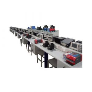
- Description
- Inquiry
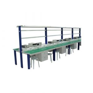
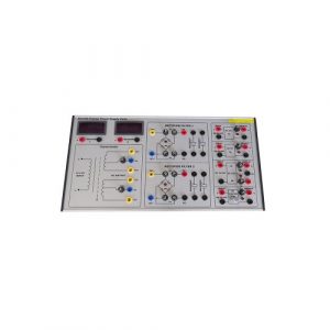
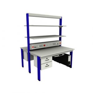
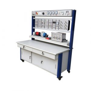
TB230621S05 Innovative RF Communication Training System Educational Lab Equipment Electrical Laboratory Equipment
Product description
The training system is mainly used to train students on the basis of relevant knowledge, through RF design software simulation design, correlation of performance index of related devices, assembly and debugging of RF circuit layout, unit circuit performance test, system gain matching adjustment and other training, so that students can deeply understand the influence of RF system distribution parameters, device characteristics and impedance matching on the communication system, and train students to learn to design and debug RF circuits. Product composition
It mainly consists of RF transmission system and RF receiving system:
- RF transmission system:
Including: Local oscillator (PLL phase-locked oscillator), up-converter, band-pass filter, adjustable gain amplification attenuator, power amplifier 1, power amplifier 2, transmitting antenna etc., realize the signal moving from IF to RF. 2. RF receiving system:
It’s the foundation of the whole communication receiving system. The complete RF receiving chain includes the receiving antenna, band-pass filter, low noise amplification, adjustable gain amplification, oscillator, mixer, and low-pass filter, to achieve the RF signal to IF signal movement, and then through the analog-digital conversion into the digital system for further processing.
Technical parameters
- Low noise amplifier (general type)
- Working frequency range: 0.5Ghz-1.5Ghz
- Noise figure: 2.5dB
- Gain: >40dB
- Maximum output power: 10dBm
- Frequency source local oscillator 1 (PLL+VCO)
- Output frequency range: 350MHz-1800GHz
- Maximum output power: +10dBm
- Phase noise: <-110dBc/Hz@100kHz
- Stabilization time: 400us
- Output frequency stray: <-70dBc
- Variable gain amplification attenuator
- Working frequency: 10Mhz-3GHz
- Gain adjustment range: -34dB~+22dB
- Frequency Source Local Oscillator 2 (PLL+VCO)
- Output frequency range: 2050MHz-2450GHz
- Maximum output power: +10dBm
- Phase noise: <-105dBc/Hz@100kHz
- Stabilization time: 400us
- Output frequency stray: <-70dBc
- Power Amplifier
- Output frequency range: 0.5GHz-1.5GHz
- 1dB power compression point: +18dBm
- Gain: > 30dB
- Working voltage: 5V
- Transmitting chain up-converter
- RF and local oscillator working frequency range: 50MHzHz-1.6GHz
- IF working frequency range: 20MHz-1000MHz
- Frequency conversion insertion loss: 9dB
- Local oscillator – RF isolation: 35dB
- Local oscillator – IF isolation: 30dB
- Receive chain down-converter
- RF and local oscillator working frequency range: 300MHzHz-2.4GHz
- IF working frequency range: DC-700MHz
- Frequency conversion insertion loss: 6dB
- Local oscillator – RF isolation: 35dB
- Local oscillator – IF isolation: 25dB
- Low noise amplifier (special type)
- Working frequency range: 900MHz±20MHz
- Noise figure: 0.3dB
- Gain: >15dB
- Maximum output power: 0dBm
- Power amplifier (special type)
- Working frequency range: 900MHz±20MHz
- 1dB power compression point: 33dBm (2W)
- Gain: >18dB
- Efficiency: > 60%
- DC bias working point: Vgs = 1.8V; Vds = 28V
- Transceiver antenna
- Working frequency range: 900MHz±10MHz
- Gain:>3dBi
- Polarization: Linear polarization
Basic experiments
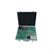
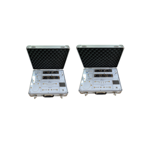
The main content of this experiment box is to train students’ design and debugging ability of RF circuit, and can demonstrate the design and debugging process of each module mentioned above.



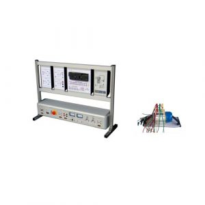
-300x300.jpg)
